A groundbreaking materials science discovery by Chinese researchers has unveiled unprecedented possibilities for revolutionary data storage technology that could transform artificial intelligence hardware. Scientists from the Institute of Physics at the Chinese Academy of Sciences have successfully identified and manipulated previously unknown atomic-scale structures within fluorite ferroelectric crystals—materials extensively used in microelectronics since the 2010s.
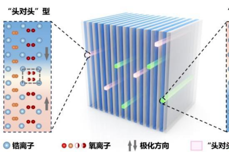
The research team, after eight years of dedicated investigation, challenged conventional scientific understanding by demonstrating that what were traditionally considered two-dimensional domain walls within these crystals are actually one-dimensional linear structures measuring mere atoms in width. These ultratiny ‘linear walls,’ approximately one hundred-thousandth the diameter of a human hair, represent a fundamental reimagining of how information can be stored at the atomic level.
Crucially, the researchers discovered that these nanometer-scale lines maintain remarkable stability through interactions with naturally occurring oxygen defects within the crystal lattice. These atomic imperfections function as microscopic anchors, preventing the structures from dissipating due to electrical forces—a critical requirement for practical data storage applications.
Using advanced electron microscopy techniques, the team achieved unprecedented atomic-scale observation and control over these linear structures. By applying localized electric fields, they demonstrated the ability to create, reposition, and erase these atomic features on demand, establishing the theoretical framework for future storage devices.
According to Dr. Zhong Hai, the study’s lead author and associate professor at Ludong University, this discovery could enable storage densities approximately 600 times greater than current technologies. This translates to potentially storing 20 terabytes of information within a single square centimeter—equivalent to fitting 10,000 high-definition movies in an area no larger than a postage stamp.
The implications for artificial intelligence development are particularly significant, as these structures could enable the creation of AI chips with dramatically enhanced processing capabilities, reduced energy consumption, and substantially higher component density. However, researchers emphasize that practical implementation remains several years away, requiring solutions to engineering challenges including electrode design for localized field control.
Published in the prestigious journal Science, this fundamental research opens new pathways in materials science while potentially laying the groundwork for a new generation of ultra-efficient computing hardware.